How Siemens is Using AI to Revolutionize Semiconductor and PCB Design
In today’s hyper-competitive technology landscape, the semiconductor and printed circuit board (PCB) industries sit at the very heart of innovation. These components serve as the critical backbone of modern electronic devices, enabling everything from smartphones and electric vehicles to industrial automation systems and advanced medical equipment. The escalating demand for greater computing power, energy efficiency, and miniaturization has driven unprecedented complexity in semiconductor and PCB design processes. Moreover, market expectations for accelerated time-to-market and reduced development costs place immense pressure on design teams to deliver flawless products under increasingly tight timelines.
This complex environment necessitates transformative innovations in how electronic systems are conceived, designed, and brought to production. Against this backdrop, Siemens has strategically embraced artificial intelligence (AI) technologies to “turbocharge” its semiconductor and PCB design capabilities. This initiative is not a mere incremental improvement; it represents a fundamental shift in the way electronic design automation (EDA) and manufacturing workflows are structured and executed.
Semiconductor and PCB design workflows have traditionally relied on a combination of highly skilled engineers, rule-based software tools, and iterative testing cycles. While this approach has served the industry well for decades, it increasingly struggles to keep pace with the growing intricacies of modern electronic systems. As designs push the boundaries of scale and performance, the number of possible configurations, interdependencies, and verification steps grows exponentially. Manual intervention and conventional automation techniques are no longer sufficient to manage this complexity with the required speed and accuracy.
AI offers a compelling solution to these challenges. By leveraging machine learning (ML), deep learning (DL), and other AI methodologies, Siemens aims to revolutionize design workflows by automating labor-intensive tasks, optimizing design parameters in ways that human engineers cannot, and providing predictive insights that improve quality and yield. In doing so, Siemens seeks to enable design teams to shift from reactive problem-solving to proactive innovation.
Siemens’ deployment of AI within its design software portfolio is strategically aligned with its broader digitalization strategy, encapsulated in the Siemens Xcelerator platform. Xcelerator provides a comprehensive suite of digital tools and services that integrate product lifecycle management (PLM), EDA, simulation, and manufacturing execution systems (MES). By embedding AI throughout this ecosystem, Siemens empowers customers to achieve new levels of efficiency, agility, and product innovation.
The term “turbocharging” in this context is not hyperbole. Initial deployments of Siemens’ AI-enhanced design tools have demonstrated dramatic reductions in design cycle times—up to 70% in certain workflows—while simultaneously improving design quality and manufacturability. These results underscore the transformative potential of AI in reshaping the future of semiconductor and PCB design.
Furthermore, Siemens’ initiative is particularly timely. The industry faces acute shortages of skilled engineering talent, while the pace of technological change continues to accelerate. AI-enabled design tools can help bridge this gap by augmenting human expertise and enabling less-experienced engineers to contribute effectively to complex design projects. This democratization of design capability is poised to have far-reaching implications for the industry’s talent dynamics.
Another critical driver for AI adoption is the growing importance of first-pass success in manufacturing. Each design iteration, or “re-spin,” incurs significant time and cost penalties, particularly in advanced semiconductor processes and multilayer PCB fabrication. Siemens’ AI-driven solutions aim to minimize re-spins by improving design accuracy and manufacturability from the outset, thereby enhancing profitability and market responsiveness for customers.
Finally, Siemens’ AI strategy is not pursued in isolation. It builds upon decades of domain expertise, extensive industry partnerships, and a robust foundation of validated design data. This unique combination of AI capabilities and domain knowledge positions Siemens as a formidable leader in the evolving landscape of AI-driven electronic design.
As this blog will explore, Siemens’ integration of AI into semiconductor and PCB design workflows is set to redefine industry best practices. In the sections that follow, we will examine the technical foundations of these AI innovations, real-world use cases and results, broader business implications, and Siemens’ future roadmap in this exciting and rapidly evolving field.
Technical Foundations
The deployment of artificial intelligence (AI) by Siemens to enhance semiconductor and PCB design is built upon a sophisticated technical foundation that integrates advanced machine learning (ML), deep learning (DL), and data-driven automation across the electronic design automation (EDA) workflow. This section provides a comprehensive overview of the methodologies, technologies, and platforms that underpin Siemens’ AI-powered design capabilities, highlighting how these innovations fundamentally transform design practices.
AI Methods & Workflows
At the core of Siemens’ AI-driven approach is the application of machine learning algorithms to automate and optimize various aspects of the design process. Traditional EDA workflows are largely deterministic, relying on rule-based engines and manual tuning to achieve design goals. While effective to a degree, these methods become increasingly inefficient as design complexity scales. In contrast, AI introduces adaptability and predictive intelligence into the process.
Supervised learning plays a central role in Siemens’ methodology. Historical design data, including layout configurations, component placements, electrical performance metrics, and manufacturing outcomes, are used to train models capable of recognizing optimal design patterns and flagging potential issues. These models continuously improve as they are exposed to more data, enabling them to refine their recommendations and predictions over time.
Deep learning techniques, particularly convolutional neural networks (CNNs), are employed for tasks that involve complex spatial relationships, such as PCB trace routing and semiconductor floor-planning. By interpreting design layouts as visual patterns, CNNs can identify routing paths that minimize signal integrity issues, electromagnetic interference, and thermal hotspots.
Generative design—a form of AI-driven co-creation—is also an integral component. In generative workflows, AI systems propose novel design configurations based on high-level objectives specified by engineers. For example, given constraints related to performance, power consumption, and manufacturability, the AI can generate multiple layout alternatives that meet or exceed these targets. Engineers can then evaluate and refine these suggestions, resulting in faster iterations and more innovative solutions.
Another significant advancement is the use of reinforcement learning (RL) in iterative optimization processes. In RL, AI agents learn to improve design outcomes by receiving feedback on the performance of their actions. For instance, an RL agent might adjust routing strategies based on feedback from signal integrity simulations, progressively refining its approach to achieve optimal results.
By embedding these AI techniques within the EDA workflow, Siemens enables a paradigm shift from manual, iterative design practices to data-driven, automated processes. This transformation is not merely about accelerating existing workflows—it fundamentally enhances design quality and expands the range of feasible solutions.
Siemens’ Specific Stack
Siemens’ AI deployment is deeply integrated within its broader digitalization strategy, particularly through the Siemens Xcelerator portfolio. Xcelerator is an open digital business platform that unifies Siemens’ comprehensive suite of software, hardware, and services, providing a cohesive environment for AI-enhanced design.
Within this ecosystem, several key platforms serve as the backbone of Siemens’ AI-driven design capabilities:
- Simcenter: A multi-physics simulation platform that enables predictive engineering. Simcenter’s AI-enhanced features allow designers to rapidly explore the design space and optimize performance across electrical, thermal, mechanical, and acoustic domains.
- Calibre: A suite of IC verification tools that incorporate AI-driven design rule checking (DRC) and layout versus schematic (LVS) verification. AI models assist in identifying and prioritizing violations, significantly reducing verification time and enhancing first-pass success rates.
- Mentor Graphics (now Siemens EDA): Siemens leverages its Mentor Graphics acquisition to provide industry-leading EDA solutions for PCB and semiconductor design. AI capabilities within this suite include automated placement and routing, manufacturability analysis, and intelligent design optimization.
A critical enabler of these AI capabilities is Siemens’ sophisticated data infrastructure. Design data from millions of prior projects—encompassing both successes and failures—are systematically aggregated, anonymized, and used to train AI models. This vast repository of validated design knowledge provides a robust foundation for model training, ensuring that AI recommendations are both reliable and contextually relevant.
The AI models themselves are continuously refined through closed-loop feedback systems. As users interact with AI-driven tools and validate outcomes through simulation and manufacturing, new data is generated that feeds back into the model training process. This iterative loop ensures that Siemens’ AI capabilities evolve in tandem with emerging design trends and customer needs.
Furthermore, Siemens’ AI solutions are designed for seamless integration with existing EDA workflows. Recognizing that many organizations have substantial investments in traditional design tools and processes, Siemens emphasizes interoperability and flexibility. AI-enhanced features can be adopted incrementally, allowing design teams to realize immediate benefits without overhauling their entire toolchain.
To illustrate the impact of Siemens’ AI integration on design efficiency, the following chart compares the time required for key design phases using traditional methods versus AI-enhanced workflows:
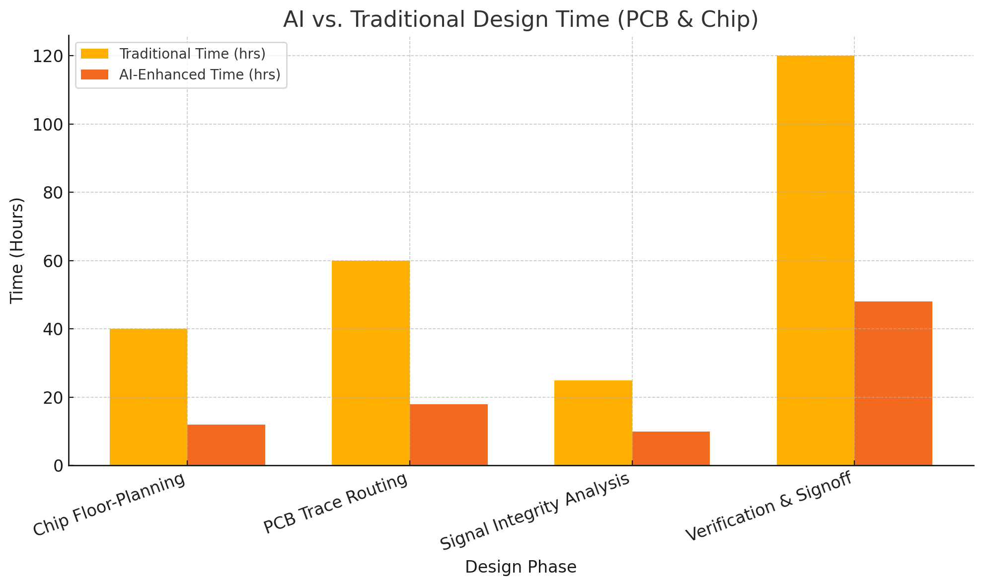
This dramatic reduction in design cycle times not only accelerates time-to-market but also allows design teams to explore a broader range of design alternatives, leading to better optimized and more innovative products.
With a robust technical foundation in place, Siemens is driving tangible improvements across semiconductor and PCB design processes.
Use Cases & Demonstrations
The integration of artificial intelligence (AI) within Siemens’ electronic design automation (EDA) suite has begun to yield tangible benefits across both semiconductor and printed circuit board (PCB) design domains. Moving beyond theoretical capabilities, Siemens’ AI-powered tools are demonstrating measurable improvements in design speed, quality, manufacturability, and first-pass success rates. This section explores several key use cases and real-world demonstrations that underscore the transformative potential of AI in electronic design workflows.
Semiconductor Design Acceleration
One of the most significant applications of AI in Siemens’ portfolio is in semiconductor floor-planning and layout optimization. These stages are critical to the overall performance, power efficiency, and manufacturability of integrated circuits (ICs). Traditionally, floor-planning has been a labor-intensive process requiring extensive manual effort and iterative tuning by highly skilled engineers. The introduction of AI fundamentally alters this landscape.
Using deep learning models trained on extensive historical floor-planning data, Siemens’ AI tools can rapidly generate optimized layouts that balance a wide range of design constraints, including timing closure, area utilization, heat dissipation, and power consumption. These models analyze millions of potential component placements and interconnect configurations, identifying solutions that would be impractical for human engineers to manually evaluate.
In one demonstration project involving an advanced system-on-chip (SoC) design, Siemens’ AI-driven floor-planning reduced layout cycle times by 70%. What previously required over 40 engineer-hours of manual effort was completed in less than 12 hours with AI assistance. Moreover, the resulting layout exhibited improved timing margins and reduced parasitic capacitance, contributing to both higher performance and lower power consumption.
Another critical area of semiconductor design where AI has proven highly effective is in verification and design-for-manufacturability (DFM) analysis. Verification is often the most time-consuming phase of the design process, involving extensive simulation and testing to ensure functional correctness and compliance with manufacturing constraints. Siemens’ Calibre suite now incorporates AI models that intelligently prioritize verification tasks based on historical outcomes and known risk areas. This targeted approach reduces unnecessary computational effort and accelerates time to signoff.
In a leading-edge application node project, AI-enhanced verification workflows achieved a 60% reduction in total verification time. Importantly, these improvements did not come at the expense of quality—first-pass silicon success rates actually increased due to more effective detection of critical issues during pre-silicon validation.
Yield optimization represents yet another powerful use case. AI models trained on fab data can predict potential yield detractors based on layout characteristics, enabling designers to proactively adjust designs before tape-out. This predictive capability reduces costly re-spins and improves overall manufacturing efficiency.
PCB Design Improvements
Printed circuit board (PCB) design is another domain where Siemens’ AI capabilities are driving substantial advancements. The process of routing signal traces across multilayer PCBs, while ensuring compliance with electrical performance and manufacturability requirements, is notoriously complex. AI-driven routing engines leverage deep learning models to automate much of this process, dramatically accelerating design cycles.
In a recent demonstration involving a 12-layer automotive PCB with stringent electromagnetic compatibility (EMC) and thermal performance requirements, Siemens’ AI-enhanced routing engine reduced routing time from 60 hours to just 18 hours. The AI-generated routing solutions not only met all electrical performance targets but also exhibited improved manufacturability metrics, such as reduced via count and optimized trace widths for better signal integrity.
Beyond routing, AI is also improving component placement optimization. Traditional placement algorithms often struggle with complex trade-offs involving thermal management, mechanical constraints, and serviceability. Siemens’ generative design tools can propose placement strategies that simultaneously address these multiple objectives, leading to more robust and maintainable designs.
Signal integrity (SI) and power integrity (PI) analysis, critical for ensuring reliable high-speed operation, also benefit from AI. Siemens’ AI models can predict potential SI/PI issues early in the design cycle, allowing engineers to make proactive adjustments. This early detection capability reduces the need for late-stage rework and enhances first-pass success.
To quantify the impact of AI integration on design quality, the following chart illustrates reductions in error rates and re-spin frequency observed in AI-enhanced workflows:

These results clearly demonstrate that AI integration not only accelerates design workflows but also enhances design quality, leading to fewer errors and higher first-pass success rates.
To further illustrate the practical benefits of AI deployment across different design areas, the following table summarizes real-world case study outcomes:
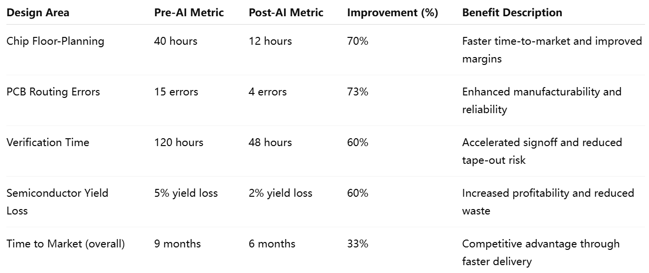
These examples underscore the multifaceted value of AI in electronic design. By automating routine tasks, optimizing complex trade-offs, and providing predictive insights, Siemens’ AI-powered tools enable design teams to achieve superior outcomes with less effort and shorter timelines.
Broader Implications
The use cases and demonstrations outlined above highlight not only the immediate benefits of AI integration but also its potential to fundamentally reshape industry practices. By reducing the barriers to high-quality design, AI democratizes access to advanced capabilities, allowing smaller design teams and less-experienced engineers to contribute meaningfully to complex projects.
Moreover, as AI models continue to improve through ongoing learning and expanded data sets, their ability to drive innovation will only increase. Siemens’ AI-powered design tools are already enabling new product architectures and performance levels that would be difficult, if not impossible, to achieve through traditional methods alone.
In sum, the practical demonstrations of Siemens’ AI-driven EDA tools make a compelling case for broader industry adoption.
Business & Industry Impact
The deployment of artificial intelligence (AI) across Siemens’ semiconductor and PCB design platforms has implications that extend far beyond technical enhancements alone. While dramatic gains in efficiency, quality, and innovation capacity have already been demonstrated at the engineering level, the broader impacts on Siemens’ competitive positioning, customer value proposition, and industry dynamics are equally profound. This section examines the multifaceted business and industry implications of Siemens’ AI initiative, from strategic benefits to customers, to potential shifts across the global EDA and electronics design landscape, as well as the challenges and considerations that accompany such a profound transformation.
Strategic Benefits for Siemens & Users
Siemens’ investment in AI-driven EDA tools is not an isolated technical project; rather, it forms an integral part of the company’s broader strategic vision to lead the digital transformation of industry. Through its Xcelerator platform and EDA portfolio, Siemens is positioning itself as a key enabler of intelligent, data-driven design and manufacturing ecosystems.
One of the most immediate strategic benefits for Siemens lies in competitive differentiation. The EDA space is dominated by a few major players—Synopsys, Cadence, Siemens EDA (formerly Mentor Graphics), and emerging AI-first challengers. By embedding AI deeply within its existing, highly trusted toolsets, Siemens offers an evolutionary path for customers: they can adopt cutting-edge AI capabilities without abandoning familiar workflows or risking business continuity. This “incremental innovation” strategy allows Siemens to expand its market share while reducing switching friction for current customers.
Furthermore, AI capabilities generate a powerful network effect: the more designs that flow through Siemens’ AI-enhanced tools, the richer the training data becomes, further improving model accuracy and predictive power. This virtuous cycle strengthens customer loyalty and makes Siemens’ platform increasingly indispensable over time.
For Siemens’ customers—semiconductor companies, OEMs, EMS providers, and system integrators—the benefits are equally compelling:
- Reduced time-to-market: AI-driven acceleration across all phases of design shortens development cycles, allowing companies to capitalize on market opportunities more quickly.
- Cost savings: Lower engineering effort, reduced re-spins, and improved yield directly translate into lower design and manufacturing costs.
- Improved product quality: Higher first-pass success rates and better design optimization lead to more reliable, higher-performing products.
- Talent leverage: By augmenting human expertise, AI tools enable less-experienced engineers to perform at a higher level, mitigating the industry-wide shortage of senior design talent.
- Increased innovation capacity: With mundane and repetitive tasks automated, engineering teams can redirect their focus toward higher-value creative work, driving product differentiation.
Siemens’ AI-driven tools also align closely with broader megatrends in the electronics industry, such as the rise of heterogeneous integration, advanced packaging, and system-in-package (SiP) architectures. These complex design domains present challenges that exceed the capabilities of traditional EDA tools—making AI an essential enabler of next-generation products.
Industry-wide Implications
Siemens’ success in applying AI to EDA is already prompting significant shifts across the global design industry. The broader implications can be analyzed across several dimensions:
Acceleration of AI adoption in EDA: Siemens’ leadership is intensifying the competitive race among EDA vendors to deliver AI-enhanced solutions. What was once an experimental feature set is rapidly becoming an industry standard. Even conservative design organizations are beginning to view AI as a strategic necessity rather than a discretionary add-on.
Shift toward data-driven design culture: The widespread use of AI is driving cultural change within engineering teams. Design practices are evolving from intuition-based decision-making toward a more analytical, data-driven approach. Engineers increasingly rely on AI-generated insights to guide design decisions, leading to improved outcomes.
Democratization of advanced design: AI tools lower the skill barrier required to execute complex designs, enabling smaller companies and emerging markets to compete more effectively with industry giants. This democratization may lead to a broader geographic diversification of design activity, fostering innovation in new regions.
New opportunities for collaboration: As AI tools become more embedded in the design process, new modes of collaboration between human engineers and AI systems are emerging. Co-creative workflows, where AI proposes alternatives and engineers refine or select optimal solutions, are becoming the norm. This hybrid approach leverages the strengths of both human intuition and machine intelligence.
Impact on adjacent industries: Siemens’ AI-driven design technologies are also influencing adjacent sectors, such as contract manufacturing and supply chain management. Better-optimized designs lead to more predictable manufacturing outcomes, improving yield forecasting and production planning. This integration of design and manufacturing intelligence aligns with the broader trend toward digital threads and digital twins in industry 4.0 ecosystems.
Challenges & Considerations
Despite the numerous advantages of AI-driven design, several challenges and considerations must be addressed to ensure successful and responsible adoption.
Data privacy and IP protection: The effectiveness of AI models depends on access to large volumes of high-quality design data. However, this raises concerns around intellectual property (IP) protection and data privacy, particularly in industries where proprietary designs confer significant competitive advantage. Siemens mitigates these risks through rigorous data governance frameworks, anonymization techniques, and customer-controlled data-sharing options.
Model trust and explainability: For AI-generated recommendations to be actionable, engineers must understand and trust the underlying logic. Black-box AI models that lack transparency can hinder adoption. Siemens addresses this through the development of explainable AI (XAI) features that provide clear justifications for design suggestions, enabling engineers to validate AI decisions and maintain design accountability.
Integration with existing workflows: Many design organizations operate within complex toolchains and regulatory frameworks. Seamless integration of AI-enhanced features into these environments is essential to avoid disruption. Siemens emphasizes interoperability and standards-based integration to facilitate smooth adoption.
Workforce adaptation: The introduction of AI tools changes the skill profile required of design engineers. Organizations must invest in training to help engineers develop proficiency in AI-augmented workflows. Siemens supports this transition through comprehensive educational resources, workshops, and community engagement initiatives.
Regulatory and ethical considerations: As AI becomes more influential in design outcomes, regulatory frameworks may evolve to address accountability and liability issues. Siemens engages proactively with industry consortia and regulatory bodies to help shape responsible AI governance practices.
A Changing Competitive Landscape
Siemens’ AI-driven advancements are reshaping the competitive dynamics of the EDA industry. While traditional EDA leaders are responding with their own AI initiatives, the barriers to entry for new AI-first players are also being lowered. Cloud-native EDA startups leveraging AI have begun to emerge, targeting specific niches such as analog design automation, PCB optimization, or generative IC layout.
Siemens’ comprehensive approach—combining domain expertise, established customer relationships, and an open, extensible platform—positions it strongly against both incumbent rivals and emerging challengers. Its emphasis on AI as an enabler of human creativity, rather than a replacement for human expertise, resonates well with customers seeking to enhance—not disrupt—their existing engineering teams.
Moreover, Siemens’ alignment with industry megatrends—such as design for sustainability, electrification, and AI-at-the-edge—ensures that its AI-driven tools will remain relevant as the electronics industry continues to evolve.
In summary, Siemens’ deployment of AI across its semiconductor and PCB design platforms is driving profound business and industry impacts. By enhancing competitive positioning, delivering superior customer value, and reshaping industry best practices, Siemens is helping to lead the next wave of intelligent, data-driven innovation in electronic design. At the same time, responsible management of the associated challenges—ranging from data governance to workforce transformation—will be critical to realizing the full potential of this technological revolution.
Future Outlook & Roadmap
The rapid adoption of artificial intelligence (AI) within Siemens’ semiconductor and PCB design platforms marks not only a major milestone in the evolution of electronic design automation (EDA) but also the beginning of a longer, more profound transformation across the entire product development lifecycle. While the current generation of AI-driven tools already delivers impressive gains in efficiency, quality, and innovation potential, Siemens envisions an even more ambitious future in which AI becomes an intrinsic and autonomous participant in the design process. This section explores Siemens’ forward roadmap, broader trends shaping the AI-driven design landscape, and the emerging possibilities that may redefine the future of electronics innovation.
Siemens’ Forward Roadmap
Siemens has articulated a clear and strategic vision for the future development of its AI-enhanced EDA capabilities, which can be grouped into three key areas: expanding technical scope, deepening AI-human collaboration, and enhancing ecosystem integration.
Expanding technical scope: One of Siemens’ immediate priorities is to extend AI-driven capabilities into increasingly advanced and emerging design domains. Current AI tools already excel at floor-planning, routing, verification, and yield optimization. The next phase will target more complex challenges such as:
- Generative chip design: Moving from AI-assisted layouts to AI-generated architectures that propose entirely novel configurations optimized across multiple physical domains (electrical, thermal, mechanical).
- Advanced packaging and 3D ICs: Applying AI to address the unprecedented complexity of heterogeneous integration, including system-in-package (SiP), chiplet-based architectures, and stacked 3D ICs.
- Multi-physics optimization: Leveraging AI to optimize designs across multiple interacting physics domains, balancing electrical, thermal, mechanical, and reliability constraints in a unified workflow.
Deepening AI-human collaboration: Siemens recognizes that the most effective AI deployment will not replace human designers but will augment and amplify their capabilities. The company’s roadmap emphasizes the development of:
- Interactive AI agents: Tools that engage engineers in real-time dialogue, suggesting design alternatives, explaining trade-offs, and adapting to engineer feedback.
- Personalized AI models: Adaptive AI systems that learn individual engineers’ preferences and organizational best practices, providing customized design guidance.
- Explainable AI: Continuing to enhance the transparency and interpretability of AI recommendations, building engineer trust and facilitating broader adoption.
Enhancing ecosystem integration: Finally, Siemens is committed to embedding AI-driven design within the broader digital engineering ecosystem. This includes:
- Integration with digital twins: Closing the loop between design, simulation, and real-world performance data to enable continuous improvement of both designs and AI models.
- Cloud-based collaboration: Expanding cloud-native AI tools that support global, distributed engineering teams and enable seamless design collaboration.
- Open data and standards: Promoting interoperability through open APIs and support for industry standards, allowing customers to integrate Siemens’ AI tools into their heterogeneous toolchains.
Together, these roadmap priorities reflect Siemens’ holistic approach to AI-driven innovation—an approach that balances technical ambition with a pragmatic focus on customer needs, human factors, and ecosystem dynamics.
Broader AI-Driven Design Horizon
Looking beyond Siemens’ internal roadmap, the broader landscape of AI-driven design is poised for even more radical evolution in the years ahead. Several emerging trends and technological frontiers are likely to redefine what is possible:
Autonomous design systems: As AI capabilities continue to mature, we may see the emergence of fully autonomous design systems that can generate entire product designs from high-level functional specifications. In this paradigm, human engineers would define what a product must do, and AI systems would determine how to implement it—handling architecture, component selection, layout, verification, and optimization with minimal human intervention.
AI for sustainability: Environmental considerations are becoming a central concern in electronics design. Future AI tools will increasingly optimize for energy efficiency, material usage, recyclability, and carbon footprint, helping companies meet aggressive sustainability targets.
Interdisciplinary design convergence: The integration of AI across traditionally siloed disciplines—electronics, mechanics, software, materials—will enable more holistic, system-level optimization. Siemens is well-positioned to lead this convergence through its Xcelerator platform, which spans multiple engineering domains.
New frontiers in quantum, photonics, and bioelectronics: AI-driven design will be essential in emerging fields where complexity vastly exceeds human cognitive capacity. Siemens and its partners are beginning to explore how AI can accelerate innovation in areas such as quantum computing hardware, integrated photonics, and bioelectronic interfaces.
AI self-improvement: Meta-learning techniques—AI systems that learn how to improve their own learning algorithms—will enable even faster progress. Siemens’ commitment to closed-loop feedback and continuous model refinement positions it to capitalize on this next wave of AI innovation.
Closing Takeaways
Siemens’ bold deployment of AI to “turbocharge” semiconductor and PCB design is a transformative development for both the company and the broader EDA industry. It delivers immediate and measurable value through faster design cycles, higher quality outcomes, and expanded innovation capacity, while also laying the groundwork for an even more ambitious future.
By expanding technical capabilities, fostering deeper AI-human collaboration, and driving ecosystem integration, Siemens is setting the pace for the next phase of AI-driven design. In parallel, broader industry trends—including autonomous design, sustainable engineering, interdisciplinary convergence, and new application frontiers—promise to reshape the very nature of how electronics are conceived and realized.
For design organizations, the message is clear: AI is no longer a future aspiration—it is an immediate and essential enabler of competitive advantage. Those who embrace this transformation will be well-positioned to lead the next wave of innovation in electronics and beyond.
To stay informed on Siemens’ evolving AI-driven design capabilities and to explore how your organization can leverage these powerful tools, we encourage you to follow the latest updates from Siemens Xcelerator and Siemens EDA.
References
- https://www.plm.automation.siemens.com/global/en/products/eda.html
- https://press.siemens.com/global/en/pressrelease/siemens-expands-xcelerator-platform-eda-tools
- https://www.mentor.com/products/ic_nanometer_design/verification
- https://www.designnews.com/electronics-test/how-ai-speeding-semiconductor-design
- https://www.eetimes.com/how-ai-is-transforming-semiconductor-design/
- https://www.semiconductordigest.com/ai-in-eda-revolutionizing-chip-design/
- https://www.pcb007.com/index.php/article/ai-driven-advances-in-pcb-layout-design/
- https://semiengineering.com/ai-eda-turbocharging-chip-packaging-design/
- https://www.siemens.com/global/en/products/automation/topic-areas/digital-enterprise/xcelerator.html
- https://www.forbes.com/sites/forbestechcouncil/ai-and-the-future-of-semiconductor-industry